본문

교수진 정보
1세부
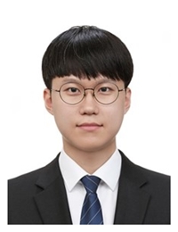
박하민 교수


Advanced Nano Device Lab
| 연구분야 | Semiconductor device based on 2D materials/ New memory device |
|---|---|
| 연구실 | 참빛관 307호 |
| 교내번호 | 02-940-8456 |
| parkhamin@kw.ac.kr | |
| Homepage | https://sites.google.com/view/park-andl/home |
교수진 소개
Career
- ‘21.03 ~ present Assistant Professor, Department of Electronic Engineering, KW Univ.
- ‘19.09 ~ ‘21.02 Staff Engineer, Samsung Electronics
- ‘15.03 ~ ‘19.08 Ph.D., School of Electrical Engineering, KAIST
- ‘13.03 ~ ‘15.02 M.S., School of Electrical Engineering, KAIST
- ‘10.02 ~ ‘13.02 B.S., School of Electrical Engineering, KAIST
Research Field
▶ Semiconductor device based on 2D materials
· Process engineering of 2D materials (CVD, ALD, plasma etching, transfer printing)
· Spectroscopic analysis on interlayer interaction (Raman, PL)
· Flexible electronics
· Device reliability (bias stress, 1/f noise)▶ New memory device
· Resistive random access memory (RRAM)
· Neuromorphic system


