본문
교수진 정보
3rd Part
Hanwool Jeong Prof.


VLSI Circuit Design Lab
| Research field | Low Voltage Digital Circuit Design/ Computation-in-Memory Circuit Design/ Low Voltage SRAM Design/ |
|---|---|
| Office | Bima-building, #604 |
| Tel. | +82-2-940-5149 |
| hwjeong@kw.ac.kr | |
| Homepage | http://sites.google.com/site/vlsicir |
교수진 소개
Career
- ‘19.09 ~ present Assistant Professor, Dept. of Electronic Engineering, KW Univ.
- ‘17.09 ~ ‘19.07 Senior Engineer, Samsung Electronics
- ‘12.03 ~ ‘17.08 Ph. D., Electrical and Electronic Engineering, Yonsei Univ.
- ‘05.03 ~ ‘12.02 B.S., Electrical and Electronic Engineering, Yonsei Univ.
Research Field
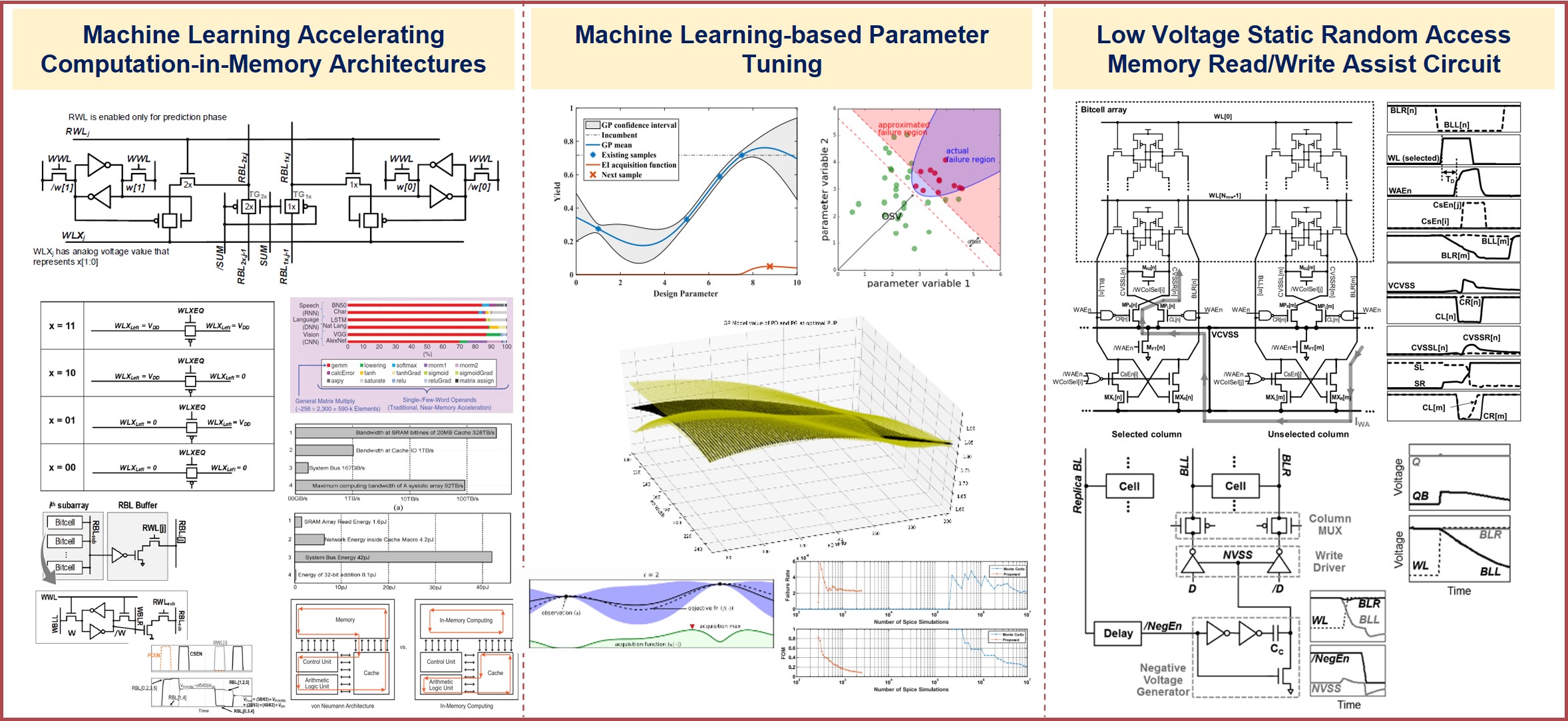
▶ Low Voltage Digital Circuit Design
· Near-threshold/Sub-threshold Flip-flop design
· Wide-range Level shifter circuit design
▶ Computation-in-Memory Circuit Design
· SRAM based in-memory computing design
· Non-volatile memory based neuromorphic circuit design
▶ Low Voltage SRAM Design
· High speed sensing circuit
· SRAM read/write assist circuit
▶ Machine Learning-based Circuit Design Automation
· Machine learning based circuit optimization
· High density memory yield estimation methodology


